Read more
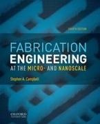
Zusatztext I like Campbell's style and enjoy reading the text. The material is appropriate for the intended audience and there are good summaries of background material. Informationen zum Autor Stephen A. Campbell is the Bordeau Professor of Electrical and Computer Engineering at the University of Minnesota and a fellow of IEEE. Klappentext Designed for advanced undergraduate or first-year graduate courses in semiconductor or microelectronic fabrication, Fabrication Engineering at the Micro- and Nanoscale, Fourth Edition, covers the entire basic unit processes used to fabricate integrated circuits and other devices. With many worked examples and detailed illustrations, this engaging introduction provides the tools needed to understand the frontiers of fabrication processes. Zusammenfassung Designed for advanced undergraduate or first-year graduate courses in semiconductor or microelectronic fabrication, Fabrication Engineering at the Micro- and Nanoscale, Fourth Edition, covers the entire basic unit processes used to fabricate integrated circuits and other devices. Inhaltsverzeichnis * = This section provides background material. ** = This section contains advanced material and can be omitted without loss of the basic content of the course. PART I. OVERVIEW AND MATERIALS Chapter 1. An Introduction to Microelectronic Fabrication 1.1 Microelectronic Technologies: A Simple Example 1.2 Unit Processes and Technologies 1.3 A Roadmap for the Course 1.4 Summary Chapter 2. Semiconductor Substrates 2.1 Phase Diagrams and Solid Solubility* 2.2 Crystallography and Crystal Structure* 2.3 Crystal Defects 2.4 Czochralski Growth 2.5 Bridgman Growth of GaAs 2.6 Float Zone and Other Growth 2.7 Wafer Preparation and Specifications 2.8 Summary and Future Trends Problems References PART II. UNIT PROCESSES I: HOT PROCESSING AND ION IMPLANTATION Chapter 3. Diffusion 3.1 Fick's Diffusion Equation in One Dimension 3.2 Atomistic Models of Diffusion 3.3 Analytic Solutions of Fick's Law 3.4 Diffusion Coefficients for Common Dopants 3.5 Analysis of Diffused Profiles 3.6 Diffusion in SiO 3.7 Simulations of Diffusion Profiles 3.8 Summary Problems References Chapter 4. Thermal Oxidation 4.1 The Deal-Grove Model of Oxidation 4.2 The Linear and Parabolic Rate Coefficients 4.3 The Initial Oxidation Regime 4.4 The Structure of SiO2 4.5 Oxide Characterization 4.6 The Effects of Dopants During Oxidation and Polysilicon Oxidation 4.7 Silicon Oxynitrides 4.8 Alternative Gate Insulators** 4.9 Oxidation Systems 4.10 Numeric Oxidations** 4.11 Summary Problems References Chapter 5. Ion Implantation 5.1 Idealized Ion Implantation Systems 5.2 Coulomb Scattering* 5.3 Vertical Projected Range 5.4 Channeling and Lateral Projected Range 5.5 Implantation Damage 5.6 Shallow Junction Formation** 5.7 Buried Dielectrics** 5.8 Ion Implantation Systems: Problems and Concerns 5.9 Numerical Implanted Profiles** 5.10 Summary Problems References Chapter 6. Rapid Thermal Processing 6.1 Gray Body Radiation, Heat Exchange, and Optical Absorption 6.2 High Intensity Optical Sources and Chamber Design 6.3 Temperature Measurement 6.4 Thermoplastic Stress* 6.5 Rapid Thermal Activation of Impurities 6.6 Rapid Thermal Processing of Dielectrics 6.7 Silicidation and Contact Formation 6.8 Alternative Rapid Thermal Processing Systems 6.9 Summary Problems References PART III. UNIT PROCESSES 2: PATTERN TRANSFER Chapter 7. Optical Lithography 7.1 Lithography Overview 7.2 Diffraction* 7.3 The Modulation Transfer Function and Optical Exposures 7.4 Source Systems and Spatial Coherence 7.5 Contact/Proximity Printers 7.6...

