Share
Fr. 129.00
SH Voldman, Steven H Voldman, Steven H. Voldman
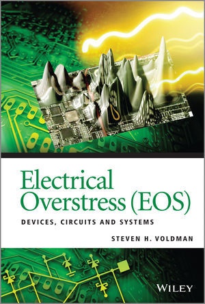
Electrical Overstress (Eos) - Devices, Circuits and Systems - Devices, Circuits and Systems
English · Hardback
Shipping usually within 1 to 3 weeks (not available at short notice)
Description
"This book addresses EOS phenomena and distinguish it from other forms of phenomena such as electrostatic discharge (ESD), latchup, and EMC events"--
List of contents
About the Author xviiPreface xixAcknowledgements xxiii1 Fundamentals of Electrical Overstress 11.1 Electrical Overstress 21.2 De-Mystifying Electrical Overstress 71.3 Sources of Electrical Overstress 81.4 Misconceptions of Electrical Overstress 101.5 Minimization of Electrical Overstress Sources 111.6 Mitigation of Electrical Overstress 111.7 Signs of Electrical Overstress Damage 121.8 Electrical Overstress and Electrostatic Discharge 141.9 Electromagnetic Interference 201.10 Electromagnetic Compatibility 211.11 Thermal Over-Stress 211.12 Reliability Technology Scaling 231.13 Safe Operating Area 261.14 Summary and Closing Comments 28References 292 Fundamentals of EOS Models 362.1 Thermal Time Constants 362.2 Pulse Event Time Constants 392.3 Mathematical Methods for EOS 422.4 The Spherical Model - Tasca Derivation 572.5 The One-dimensional Model - Wunsch-Bell Derivation 622.6 The Ash Model 682.7 The Cylindrical Model - The Arkihpov-Astvatsaturyan-Godovosyn-Rudenko Derivation 682.8 The Three-dimensional Parallelepiped Model - Dwyer-Franklin-Campbell Derivation 692.9 The Resistor Model - Smith-Littau Derivation 762.10 Instability 792.11 Electro-migration and Electrical Overstress 842.12 Summary and Closing Comments 84References 853 EOS, ESD, EMI, EMC and Latchup 873.1 Electrical Overstress Sources 873.2 EOS Failure Mechanisms 943.3 Failure Mechanism - Latchup or EOS? 973.4 Failure Mechanism - Charged Board Model or EOS? 983.5 Summary and Closing Comments 99References 994 EOS Failure Analysis 1024.1 Electrical Overstress Failure Analysis 1024.2 EOS Failure Analysis - Choosing the Correct Tool 1124.3 Summary and Closing Comments 129References 1305 EOS Testing and Simulation 1335.1 Electrostatic Discharge Testing - Component Level 1335.2 Transmission Line Pulse Testing 1405.3 ESD Testing - System Level 1435.4 Electrical Overstress Testing 1485.5 EOS Testing - Lightning 1495.6 EOS Testing - IEC 61000-4-5 1505.7 EOS Testing - Transmission Line Pulse Method and EOS 1515.8 EOS Testing - D.C. and Transient Latchup 1535.9 EOS Testing - Scanning Methodologies 1545.10 Summary and Closing Comments 161References 1616 EOS Robustness - Semiconductor Technologies 1666.1 EOS and CMOS Technology 1666.2 EOS and RF CMOS and Bipolar Technology 1806.3 EOS and LDMOS Power Technology 1866.4 Summary and Closing Comments 194References 1957 EOS Design - Chip Level Design and Floor Planning 1967.1 EOS and ESD Co-Synthesis - How to Design for Both EOS and ESD 1967.2 Product Definition Flow and Technology Evaluation 1977.3 EOS Product Definition Flow - Constant Reliability Scaling 1997.4 EOS Product Definition Flow - Bottom Up Design 2007.5 EOS Product Definition Flow - Top Down Design 2007.6 On-Chip EOS Considerations - Bond Pad and Bond Wire Design 2027.7 EOS Peripheral I/O Floor Planning 2027.8 EOS Chip Power Grid Design - IEC Specification Power Grid and Interconnect Design Considerations 2067.9 Printed Circuit Board Design 2097.10 Summary and Closing Comments 211References 2118 EOS Design - Chip Level Circuit Design 2138.1 EOS Protection Devices 2138.2 EOS Protection Device Classification Characteristics 2138.3 EOS Protection Device - Directionality 2168.4 EOS Protection Device Classification - I-V Characteristic Type 2178.5 EOS Protection Device Design Window 2208.6 EOS Protection Device - Types of Voltage Suppression Devices 2228.7 EOS Protection Device - Types of Current-Limiting Devices 2298.8 EOS Protection - Across Board Supply and Ground Plane Using a Transient Voltage Suppression Device and Schottky Diodes 2368.9 EOS and ESD Protection Co-Synthesis Network 2378.10 Co-Synthesis of EOS in Cables and PCBs 2378.11 Summary and Closing Comments 239References 2399 EOS Prevention and Control 2409.1 Controlling EOS 2409.2 EOS Minimization 2429.3 EOS Minimization - Preventive Actions in the Design Process 2469.4 EOS Prevention - EOS Guidelines and Procedures 2469.5 EOS Prevention - Ground Testing 2479.6 EOS Prevention - Connectivity 2479.7 EOS Prevention - Insertion 2479.8 EOS and Electromagnetic Interference Prevention - Printed Circuit Board Design 2489.9 EOS Prevention - Desktop Boards 2519.10 EOS Prevention - On-Board and On-Chip Design Solutions 2529.11 High Performance Serial Buses and EOS 2579.12 Summary and Closing Comments 259References 25910 EOS Design - Electronic Design Automation 26310.1 EOS and Electronic Design Automation 26310.2 EOS and ESD Design Rule Checking 26310.3 EOS Electronic Design Automation 26610.4 Printed Circuit Board Design Checking and Verification 27010.5 EOS and Latchup Design Rule Checking 27310.6 Summary and Closing Comments 282References 28211 EOS Program Management 28511.1 EOS Audits and Manufacturing Control 28511.2 Controlling EOS in the Production Process 28711.3 EOS and Assembly Plant Corrective Actions 28711.4 EOS Audits - From Manufacturing to Assembly Control 28811.5 EOS Program - Weekly, Monthly, Quarterly, to Annual Audits 28811.6 EOS and ESD Design Release 28911.7 EOS Design, Testing and Qualification 29711.8 Summary and Closing Comments 298References 29812 Electrical Overstress in Future Technologies 30112.1 EOS Future Implications for Future Technologies 30112.2 EOS in Advanced CMOS Technology 30212.3 EOS Implications in 2.5-D and 3-D Systems 30412.4 EOS and Magnetic Recording 30912.5 EOS and Micro-Machines 31212.6 EOS and RF MEMs 31612.7 EOS Implications for Nano-Structures 31812.8 Summary and Closing Comments 322References 322Appendix A: Glossary of Terms 329Appendix B: Standards 335Index 339
Product details
| Authors | SH Voldman, Steven H Voldman, Steven H. Voldman |
| Publisher | Wiley, John and Sons Ltd |
| Languages | English |
| Product format | Hardback |
| Released | 18.10.2013 |
| EAN | 9781118511886 |
| ISBN | 978-1-118-51188-6 |
| No. of pages | 368 |
| Series |
ESD ESD |
| Subjects |
Natural sciences, medicine, IT, technology
> Technology
> Electronics, electrical engineering, communications engineering
Elektrotechnik, Elektromagnetismus, elektromagnetische Verträglichkeit, Electrical & Electronics Engineering, Elektrotechnik u. Elektronik, Schaltkreise - Theorie u. Entwurf, Circuit Theory & Design, Electromagnetic Theory, Electromagnetic Compatibility |
Customer reviews
No reviews have been written for this item yet. Write the first review and be helpful to other users when they decide on a purchase.
Write a review
Thumbs up or thumbs down? Write your own review.

